video
2dn
video2dn
Найти
Сохранить видео с ютуба
Категории
Музыка
Кино и Анимация
Автомобили
Животные
Спорт
Путешествия
Игры
Люди и Блоги
Юмор
Развлечения
Новости и Политика
Howto и Стиль
Diy своими руками
Образование
Наука и Технологии
Некоммерческие Организации
О сайте
Видео ютуба по тегу Doping In Transistor
Semiconductor Physics: Energy Bands, Doping & Transistors
What Is Doping In 1950s Transistor Materials? - Im a 50s Baby
A PNP transistor is doped such that the emitter doping is 10 times that in the base The minority ca
What Is Doping In Transistor Manufacturing? - Moments That Changed Everything
Semiconductor Series Ep.4 (Tamil): What is Doping? | அசுத்தப்படுத்தும் தொழில்நுட்பம் | ஆச்சரிய தகவல்
In Bipolar junction transistor, doping is | PGMN Solutions
BIPOLAR JUNCTION TRANSISTOR; WORKING OF TRANSISTOR; BARRIER POTENTIAL;DOPING; BREAKDOWN CURRENT-35;
In a transistor, comparing the doping of emitter, base and collector the part | PGMN Solutions
Transistor Regions Explained: Width, Doping & Characteristics | Part -1
What is a Semiconductor? | Band Gap, Doping & How Semiconductors work
IC (instigated circuit) transistor diode triode LED diode semiconductor device doping PN junction 🇮🇳
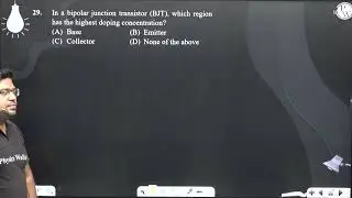
In a bipolar junction transistor (BJT), which region has the highest doping concentration?....
Легирование: важнейшая часть создания полупроводников
BJT - Bipolar Junction Transistor (Basics, Meaning, Symbols, Structure, Applications, Pros & Cons)
Microelectronics 1.1, Silicon, Doping, MOS Transistor Structure & Symbol Explained
The Doping Concept
In \( N P N \) transistor, if doping in base region is increased then collector current (A) Incr...
Concept of doping in BJT 💥l by Ravendra Yadav
Prof. Keehoon Kang, Towards the Limits of Organic Electronics: Doping Perspectives
In a transistor, the base is made very thin and lightly doped with ...
The heavily and lightly doped regions of a bipolar junction transistor are respectively (a) base ...
The part of the transistor which is heavily doped to produce large
What is Doping?| Types of Semiconductor| Class12th| CONCEPTUAL PHYSICS
Why Emitter Base Collector Doping Order is NE NB NC | Logically Explained IISc/IIT Interview Prep-3
Transistor Explanation and N, P-Type Doping, Formation of Depletion Region and NPN In Very Easy Way
Следующая страница»